My First Shitty Add On Pt2
This was going to be just a short follow up to my previous post on my shitty add on (SAO), however it’s ended up being longer than the first. I have respun the SAO to fix it’s bugs, and to optimize for production.
The changes
The following changes have been made to the board since the last revision.
The reversed connector
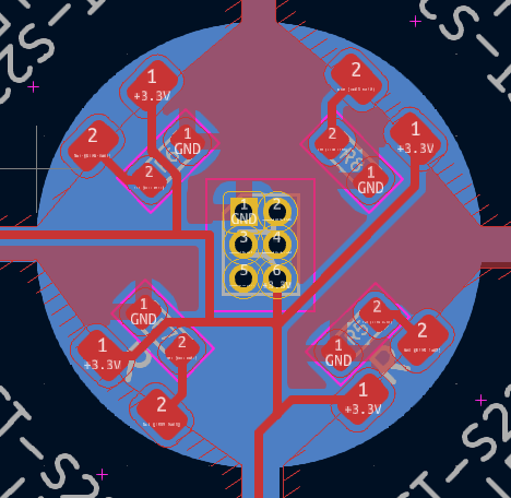
Fixing this was pretty easy, the issue was the “front” of my board in KiCad, the part with the components on, is the back of the board when in use. Pins have been corrected, power should now be good 1.
The power draw
All the LEDs on their board with their corresponding 100Ω current limiting resistors was pulling 0.26A. A bit of playing with my Digital DC Power Supply2 and the LEDs were plenty bright enough at 0.15A so a new resistor value of 180Ω was picked.
MOAR LEDs
Four more LEDs were added around the center of the board to help smooth out the light toward the center of the board. This will bring the power budget back up a bit but I think it’s worth it, and will smooth out the light especially with the new higher value resistors meaning the current LEDs will be a bit dimmer.
MOAR LEds
Panalisation
For this revision with the help of Omer I had a go at panalising the board. In this case this was primarily to remove the tooling holes, but for other projects panalising can have a significant price benefit, and is the only way with JLCPCB to get more than 30 copies of a board in one order.

The Panel Board ready for JLPCB
Experimenting with diffusers
I was planning to try some different techniques or materials for the diffuser, but the time crunch killed me so I went with the hot snot. I got a technique where I flooded the back with very hot hot-glue and then tapped the badges before it cooled to level it and help pop the bubbles.
This Time’s F*ckups
VCUTS
I panalised this for vcuts, but these are not available in JLPCBs economy option. Thankfully they converted the board to “mouse bites” for me. This won’t be quite the same edge finish but saved re-submitting the board and will be ok after a little hand finishing.
BOM
For this revision and as previously mentioned I intended to increase the value of the current limiting resistors, for the previous version Omer created my BOM file, but I made a quick change and sent this BOM to production…
| Comment | Designator | Footprint | JLCPCB Part # |
|---|---|---|---|
| J1 | C780054 | ||
| R1, R2, R3, R4, R5, R6, R7, R8, R9, R10, R11, R12, R13, R14, R15, R16, R17, R18, R19, R20, R21, R22, R23, R24 | C25744 | ||
| LED1, LED2, LED3, LED4, LED5, LED6, LED7, LED8, LED9, LED10, LED11, LED12, LED13, LED14, LED15, LED16, LED17, LED18, LED19, LED20, LED21, LED22, LED23, LED24 | C284934 |
When making the bom it turns out I can’t read JLCPCB part C284934 which is 62.5mW Thick Film Resistors ±100ppm/℃ ±1% 10kΩ 0402 Chip. It should be noted that 10kΩ is not the 150Ω that I should have selected.

Hand soldering 0402 resistors
This has led to hand soldering (at the point of writing) over 400 0402 chip resistors3. This was a very stupid and time consuming mistake. The pen marks in the photo above are my way of tracking which resistors I have successfully “fixed”. If I continue with making PCBs I think I will invest in some magnification, but for anyone else who needs to do the same, some decent flux and a nice sharp pair of tweezers are a must.
The Final Badge
You will have to wait until after DEFCON to see the final badge as they are already all packed up ready to go.
And here is the SAO living on CovertSwarms badge. The colour looked smoother in real life, googly eyes are not standard, but should be required.

SAO in it’s natural habitat